 Fraunhofer Institute for Mechanics of Materials IWM
Localized growth of silicon crystals: Fraunhofer IWM presents the »Triboepitaxy« concept
Four scientists from Freiburg have succeeded for the first time to simulate the localized growth of silicon crystals using shear-induced amorphization and recrystallization. In the future, experts could use this concept to tailor crystalline silicon structures for nanotechnology applications, such as nanoelectronics. “Triboepitaxy”, the fundamental idea that could make this possible, is presented by the team in the journal “Physical Review Letters”.
Silicon is the most important material in micro- and nanoelectronics. Yet it still takes considerable effort to fabricate crystalline silicon structures with nanoscale precision. The growth of epitaxial silicon on selected areas of a surface involves expensive and time-consuming pre-patterning steps to control the growth location. A mechanical method in which one crystal is used as a pencil to directly 'write' crystalline nanolines on another crystal entirely without pre-patterning would be a breakthrough. Thomas Reichenbach, Dr. Gianpietro Moras and Prof. Dr. Michael Moseler of the Fraunhofer Institute for Mechanics of Materials IWM, Microtribology Center µTC, in cooperation with Prof. Dr. Lars Pastewka of the Institute of Microsystems Engineering at the University of Freiburg, have now discovered something in their simulations that could make this possible in the future.
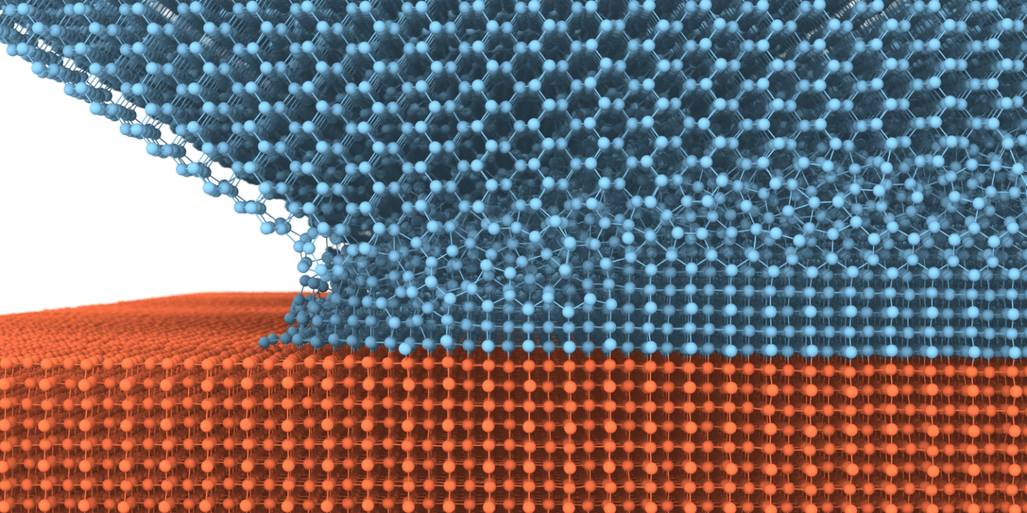
“When two silicon crystals slide against each other, an amorphous layer forms at the interface,” the tribologists explain. Normally, they say, this amorphous layer grows over time.“ However, we have found that its thickness stabilizes at a constant value at low pressure, even though new atoms are constantly entering the amorphous phase,” says Thomas Reichenbach. “This means that there must be a counteracting process in which atoms in the amorphous layer return back into the crystalline phase resulting in a steady-state thickness.”
“Triboepitaxy”: one crystal grows at the expense of another
The tribologists want to harness this newly discovered mechanical process. In simulations, they have observed that the relative orientation of the crystals is crucial. If both crystals have the same orientation, the position of the amorphous layer varies only stochastically without any discernible trend. “However, if we rotate one of the two crystals so that the shear stress in the two crystals acts along different crystallographic directions, this motion becomes directional,” explains Dr. Moras. As a result, the amorphous layer moves preferentially in one direction: one crystal grows at the expense of the other.
© Fraunhofer Institute for Mechanics of Materials IWM
In the next step, the team wanted to find out what determines which crystal grows, and which disappears. The scientists found an explanation by looking at the atomic processes: “When we apply a shear stress, there are energy differences between the two differently oriented crystals due to different elastic constants,” Reichenbach says. Simulations of a wide variety of systems showed that the crystal with the lower elastic energy density always grows. “Since it is energetically more favorable, the atoms in the amorphous phase preferentially adapt to its crystalline structure.” As a result, the other crystal - which is energetically less favorable under shear stress - is consumed. The team calls this phenomenon “triboepitaxy”.
In the future, this knowledge could find application in a nanolithography process. The tribologists propose a model experiment for this in their paper. “With a rapidly oscillating crystalline tip that is additionally moved slowly along an arbitrary path, it should be possible to write crystalline structures on another crystal,” Dr. Moras explains. “Provided the effective shear moduli of the two crystals differ.” The thickness of the crystal lines can be controlled by the number of oscillations, and the width of the trace is determined by the amplitude of the oscillations. “So far, this is all theory,” Dr. Moras said. “But it works reliably in simulations, and we hope that the idea of 'triboepitaxy' will be explored experimentally and eventually applied in the future.”
Reichenbach, T.; Moras, G.; Pastewka, L.; Moseler, M., Solid-phase silicon homoepitaxy via shear-induced amorphization and recrystallization, Physical Review Letters 127/12 (2021) 126101 1-6. Link