Fraunhofer Institute for Mechanics of Materials IWM
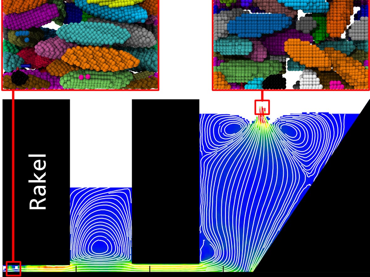
Tape casting
It used to be that numerical simulations for ceramic sheet producers were rarely used to improve the production process. For this reason, the Fraunhofer IWM developed a linked simulation model at the microstructure and tape caster level so that predictions can be made about the ceramic casting process, including the calculation of the particle orientation in the casting slurry and in the resulting product. This allows the process management for tape casting to be optimized for cost efficiency. Waste can be reduced, desired gradients in the particle distribution can be precisely adjusted or the alignment of elongated or platelet-like targeted particles can be improved or avoided – depending on the respective application.